
Picture this: On a dry winter’s day, you’re snuggled up on the couch, wearing a pair of wool socks to keep warm. Suddenly, the doorbell rings, and you rush to open the door, walking across a carpet in the process. As soon as you touch the metal doorknob, there’s an abrupt zap. Ouch! For manufacturers of electronic devices, this phenomenon of electrostatic discharge (ESD) can cause significant issues in industrial applications. In this blog post, we’ll explore how modeling and simulation can help.
Types of ESD Device Damage
The most common and visible example of an electrostatic discharge event is lightning, but not all ESD events cause a visible spark. The amount of static electric charge accumulating on an object depends on its material, surface area, and the relative humidity of its surroundings. ESD can also be caused by electrostatic induction, which occurs when the presence of an electrically charged object creates an electrostatic field around a conductive object that is isolated from the ground.

Figure 1. An ESD event with visual sparking. Photo by P. Mikołajek, licensed under the Creative Commons Attribution-Sharealike 4.0 International license, via Wikimedia Commons.
These electrostatic discharges can release anywhere from a few volts to a few kilovolts; however, even a low-voltage discharge may cause severe damage to electronic components ranging from simple diodes to complex integrated circuits. (A person can carry a charge sufficient enough to cause harm to the performance of electronic devices and components, which can lead to data loss, file corruption, and system crashes!) It’s therefore important to prevent ESD events during the manufacturing, assembling, and shipping of these devices, as well as in the finished device itself.
Understanding and Preventing ESD Damage
To avoid damage from ESD events, electronic devices and systems are required to pass a variety of tests from the component, PCB, and system levels. However, such testing can help only after the component or system is manufactured. The COMSOL Multiphysics® software enables engineers to identify ESD problems during the design stage while also providing detailed information about the electromagnetic field distribution, which is otherwise very difficult to measure accurately. This knowledge is crucial in understanding why ESD damage happens and how it can be fixed.
An ESD event may cause insulating failure or logic errors in chips. A logic error can occur when a pin meant to be in a low state (0) experiences a voltage of amplitude higher than 1.5 V for more than 1 ns or a voltage of amplitude higher than 0.3 V for more than 5 ns. This will result in the pin erroneously transferring to a high state (1).
Let’s take a look at how ESD can lead to logic errors in a microchip on a PCB.
Modeling ESD in PCBs
The RF Module, an add-on product to COMSOL Multiphysics®, has a built-in physics interface for studying ESD currents, which are usually nonlinear and require a 3D transient analysis. The Electromagnetic Waves, Transient interface includes four predefined ESD currents to cater to different testing standards and supports predefined and parameterized temporal pulse functions that are often used to describe ESD and lightning. For convenience of inspection, the pulse shapes can be immediately plotted before running the simulation to ensure that the chosen function parameters are suitable.
In this model, the ESD current has been generated using the Lumped Port feature with the extended human-body model (HBM) standard to test against the most severe conditions (Figure 2).
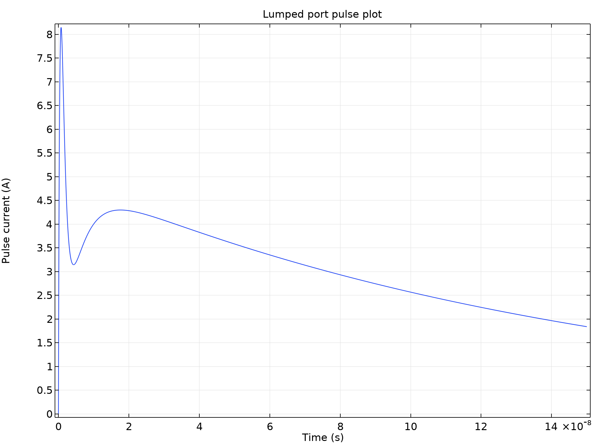
Figure 2. ESD current based on extended HBM.
Note that we won’t cover the details of how to set this model up here, but you are welcome to download the MPH file and related instructions from the bottom of this blog post.
Results
The induced voltages at two pins (1, 2) on a microchip are computed to evaluate if there will be an error due to ESD. At left below, the figure shows the induced surface current density by the ESD current at t = 1.2 ns. At right below, the figure shows the computed induced voltage at two pins (1, 2) of the chip.
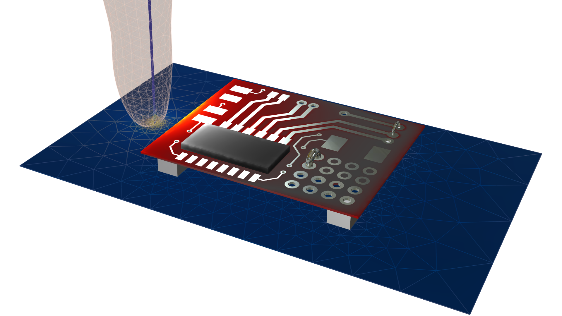
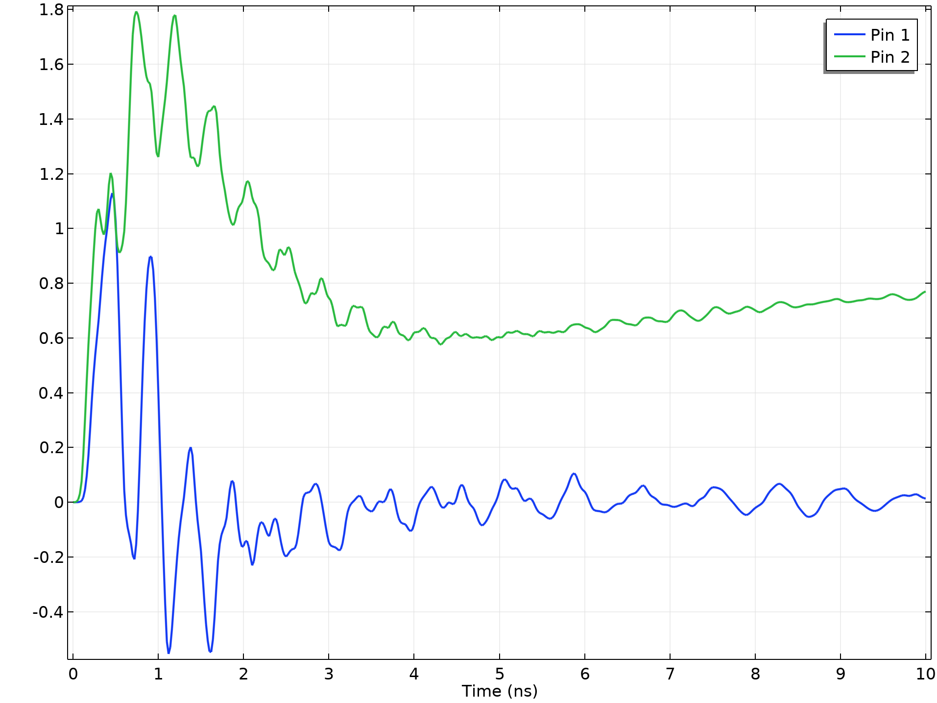
Figure 3. Induced surface current and voltage at two pins on the microchip. A fictitious fingertip is added only for visualization purposes.
As can be seen, the induced voltage at pin 2 has an amplitude higher than 1.5 V and is very likely to trigger a logic error.
The norm of surface current density, visualized on a logarithmic scale as a function of time.
Roadmap for ESD Damage Prevention
ESD is a commonly occurring phenomenon and a major source of damage and failure in electronic devices. As device sizes continue to shrink and circuit density continues to grow, it has become increasingly important for manufacturers to pay close attention to the prevention of ESD damage.
Numerical simulation provides a way to look closely inside these small devices, as well as a way to accurately model and optimize the designs before needing to build a physical prototype. It can also be used as a precompliance measure to effectively supplement testing. The passing of a simulated test can instill a high degree of confidence that a physical test will pass as well. Simulation can also offer a view of failure mechanisms and current flow and provide solution insights.
Next Steps
Ready to try this electrostatic discharge model yourself? All of the model files, including step-by-step instructions, are available for download from the Application Gallery.


Comments (0)