At the COMSOL Conference in Boston, Lam Research Corporation held a keynote talk about Moore’s law and its role in computational modeling. The keynote touched on how Moore’s law has not only impacted the advancement of simulation tools, but also how the development of these tools have themselves allowed Moore’s law to hold true. The concept was something that interested me, and I know it’s been on the minds of many electrical engineers as well. Case in point, when browsing through the November issue of IEEE Spectrum, I came across an article that discussed the current state of Moore’s law and speculated on how it may change in the coming years.
![]()
Silicon chip. Image attribution: David Carron at en.wikipedia.
Less is “Moore”
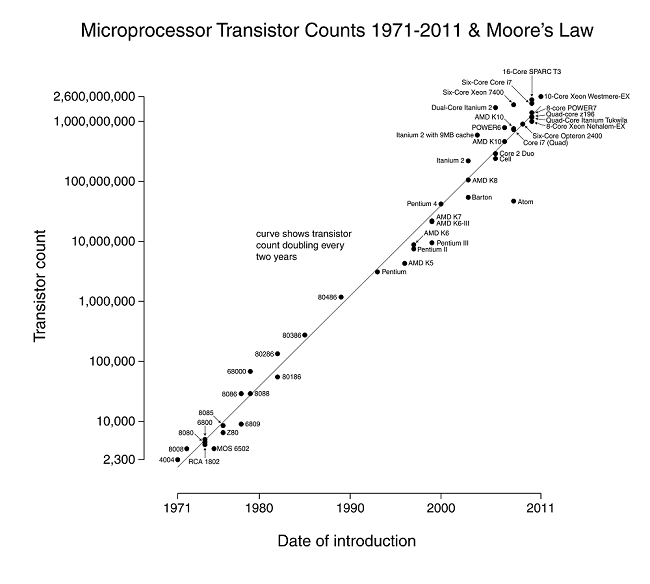
Moore’s law is named after Intel co-founder Gordon Moore, and refers to the prediction he made in the 1960’s that computing power would double every two years. So far, this prediction has held true. According to the Information Technology and Innovation Foundation, “computing power is over 1.1 million times faster today than it was 40 years ago.” This means that “less” device — i.e. smaller laptops, phones, cameras etc. — can deliver “moore” (pardon the pun) power for their size. Over the past few decades, this law has proven to be accurate to such a degree that it is talked about as if it were a “law of nature”. The almost uncanny fruition of Moore’s law can be attributed to the fact that it is now often used in the semiconductor industry for setting industry goals. However, as was presented in the IEEE Spectrum article, the way we measure the success of Moore’s law has become complicated, and has changed drastically over the course of the past decade.

Transistor counts for integrated circuits plotted against their dates of introduction (Click image to enlarge).
Image attribution: Wgsimon.
Measuring Moore’s Law
Currently, Moore’s law is “measured” by the number of transistors that can be contained within an integrated circuit. According to the article in IEEE, chips used to be able to be described by their node names, which reflected the density and number of transistors on an integrated circuit, and thereby the progression of Moore’s law from one generation to the next. However, over the past decade, these node names have begun to mean less and less. In fact, the article suggests that node names may even be chosen simply to reflect where the next generation of transistors should be. So instead of node names being given based off of key chip dimensions, such as the size and density of transistors, the transistor gate length, and the metal half pitch, the name of the device is given based on what the industry is expecting to come next.
Current chip densities (most of which are around 20-nm to 22-nm) can no longer become smaller using the same techniques as were used in the past. This is because as chips become smaller, new manufacturing processes must be developed that can in turn add additional costs to the patterning process. Smaller chip densities can even necessitate the use of additional chip features to compensate for complications that arise as the transistors become closer together and interact with one another. The article points out that these added features often negate the overall decrease in size of the chip due to the additional space needed to house the features.
The semiconductor industry has responded to this in a few different ways. One example given in the article refers to the new line of transistors by GlobalFoundries — the world’s second largest chip manufacture — that are expected to begin production in 2014. Their new integrated circuits have been named 14-nm chips, since this is the expected step after the company’s current 20-nm chip. However, the density of the chip is basically the same as that of the 20-nm chip. So what’s with the name change? As the article states, GlobalFoundaries says that they refer to them as 14-nm chips because they represent a full generation’s step in performance when compared to the previous chips. Instead of shrinking transistor size, GlobalFoundries is focusing on creating devices that exhibit the next generation of performance, not the next step in transistor density.
While this was one company’s response to the current state of the transistor industry, others are still attempting to meet the trend. Nearing the end of Moore’s law isn’t a new topic of discussion — for decades we’ve repeatedly thought we had reached the end of our ability to decrease transistor size, only to find that a new patterning process or technological advancement that allowed the trend to continue on to the next generation.
What do you think? Have we reached the “end of the shrink” or are there still more transistor density improvements to come down the line?


Comments (0)