

Surface-mount devices (SMDs) allow PCB designers to fit many components onto a PCB, allowing for a large number of functioning circuits in a small footprint. The soldering technology used to mount the SMDs places high levels of stress on the devices that can cause deformation that degrades function. Preconditioning is a process that reproduces these stresses in a controlled and repeatable manner and is performed prior to reliability testing. In this blog post, we’ll explore a model that analyzes the thermal stress and hygroscopic swelling of an SMD through the three preconditioning stages.
Surface-Mount Devices
Surface-mount devices are leadless or short-lead components that attach to the surface of a printed circuit board or base plate. The method of attaching the components is called surface mount technology (SMT), which uses soldering or dip soldering to attach the devices. This places the SMD under elevated temperatures that can deform it and hinder its ability to be attached to the PCB. To reproduce the effects of elevated temperatures, preconditioning is performed prior to reliability testing. Through finite element modeling, engineers can gain a better understanding of the effects the preconditioning process has on SMDs.
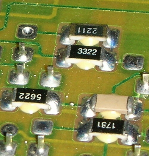
Soldered surface-mount device. This file is licensed under the Creative Commons Attribution-Share Alike 3.0 Unported, 2.5 Generic, 2.0 Generic and 1.0 Generic license, via Wikimedia Commons.
Modeling the Preconditioning Process
One example of an SMD is the insulated-gate bipolar transistor (IGBT). The Preconditioning (PRE) of Surface-Mount Devices (SMDs) model represents an IGBT module, a collection of IGBTs attached to a power semiconductor substrate. This model serves as an example of how modeling and simulation can be used to analyze the multiple solder reflow operations an SMD goes through during the board assembly process. The soldering puts the SMD under elevated temperatures, which can cause internal damage, especially if there is moisture inside the package. Preconditioning is intended to generate the stresses of board assembly before reliability testing in a controlled and repeatable way. The industry standard test method for the preconditioning sequence of SMDs used in this model is standard JESD22-A113I.
There are three main steps to the preconditioning process:
- Bake
- Moisture soak
- Reflow
If the simulated device shows excessive stress and deformation, it could indicate the need to redesign the reflow process, such as slowing the rate of temperature ramp up, or the need for alternative electromagnetic compatibility material, such as one that is less hygroscopic.
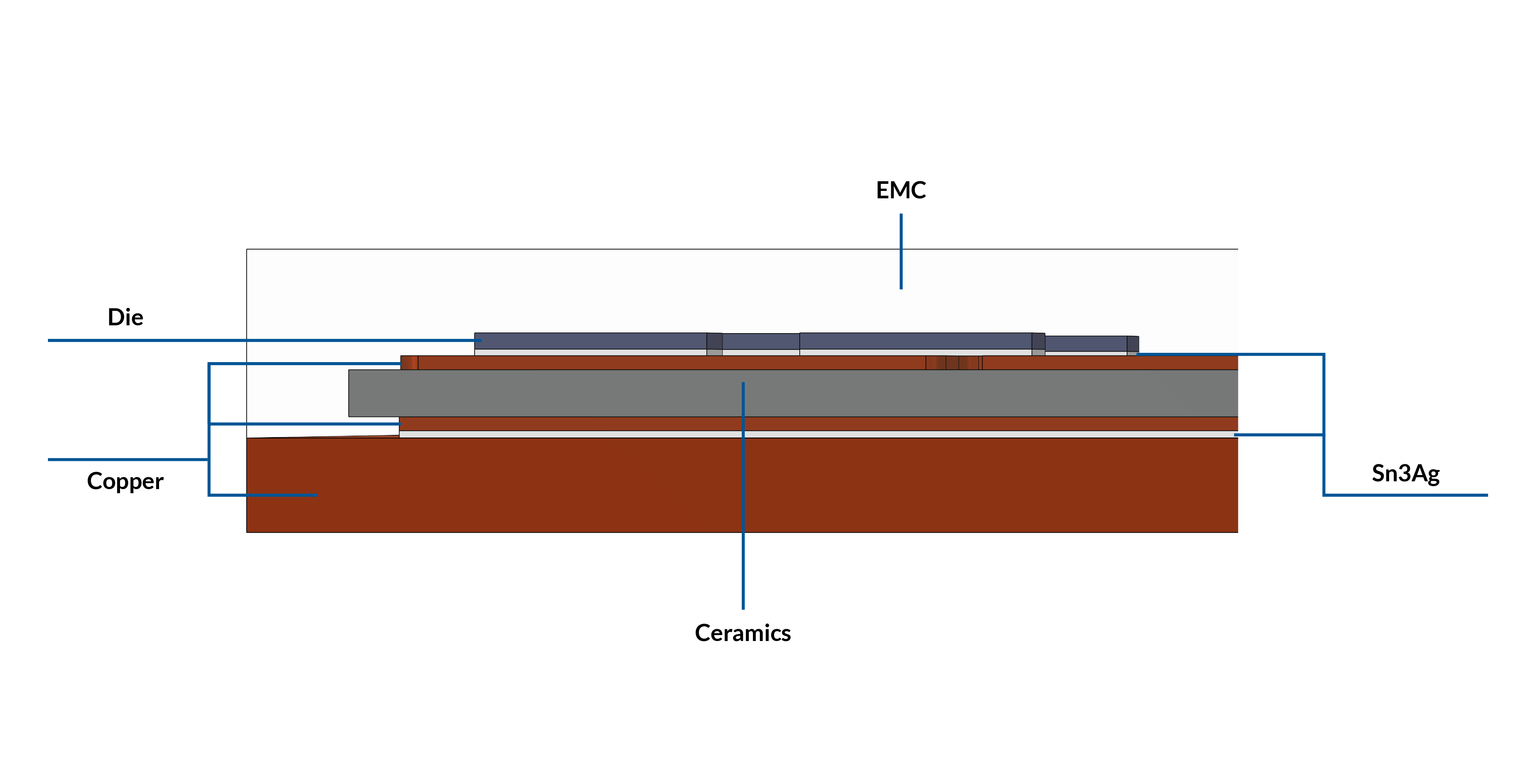
The model geometry of an IGBT module.
Bake
The first step of the preconditioning process is baking, where moisture is removed from the structure at high temperatures. The IGBT is gradually heated to ensure uniform temperature distribution and baked for 24 hours at 125°C. This step minimizes the thermal shock that occurs in the reflow stage. The initial moisture concentration is 10 mol/m3, and the concentration at the outer boundary of the plastic seal is set to 0 mol/m3. As shown below, the device deforms into a concave shape during the baking process.
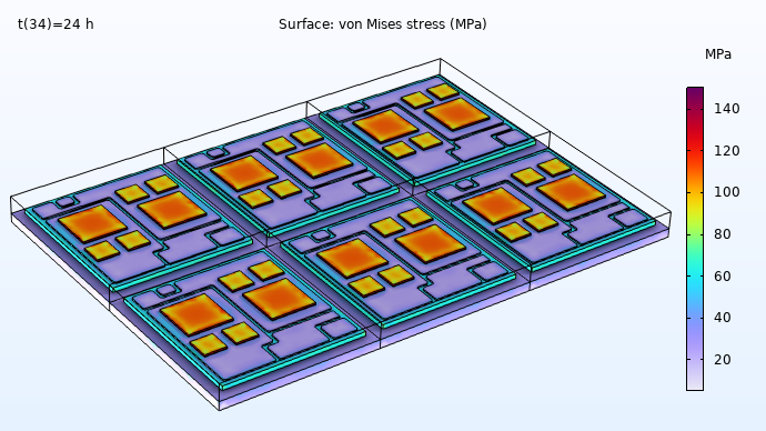
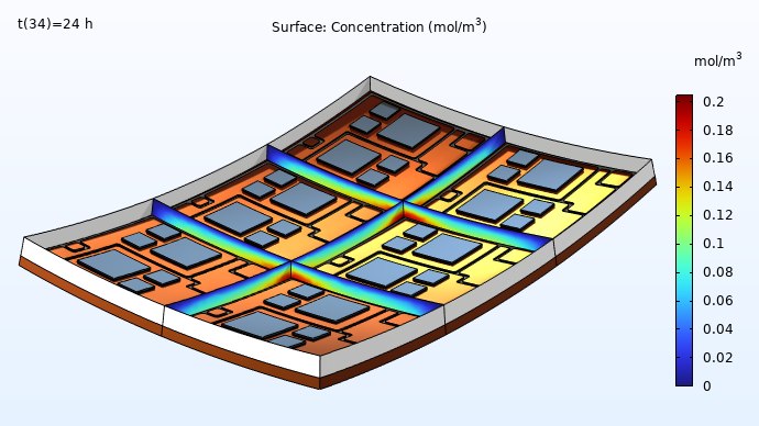
Left: Stress distribution after baking step finished. Right: Moisture concentration in the plastic seal after baking step finished (with the structure deformation shown).
An animation of the structure deformation during the baking step.
Moisture Soak
The next step in the preconditioning process measures the effects of moisture during the reflow process, as the concern is that the moisture inside the EMC layer will produce stresses during reflow and lead to reliability issues. The moisture soak following the initial bake is a way to introduce moisture into the EMC layer in a controlled manner so that whatever effects it may cause during the reflow process will be repeatable. In this case, the moisture soak process lasts 192 hours at 40°C. The structure is considered to be dry after baking, so the initial concentration is 0 mol/m3. Concentration on the outer boundary of the plastic seal is kept as 140 mol/m3, assuming the moisture is saturated at the outer boundary during the step. The IGBT deforms less than it did during the baking step, shifting into a slight convex shape.
An animation of the structure deformation during the moisture soak step.
Reflow
Reflow, or the soldering stage, raises the IGBT module temperature to the melting point of the solder paste that will be used, liquefying it. The reflow of the molten solder is what attaches the IGBT module to the PCB. The reflow test is conducted directly after the moisture soak, with the initial moisture concentration being taken from the final result of the previous soak. In this model, the reflow goes through three cycles over the course of 21 minutes, with the maximum temperature reaching 260°C. During the process, the IGBT module is deformed in a concave shape during the peak temperature and deformed in a convex manner during the reflow. This step puts the most stress on the device, and the model helps predict both the locations and the levels of stress.
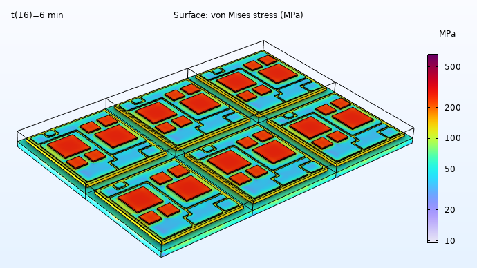
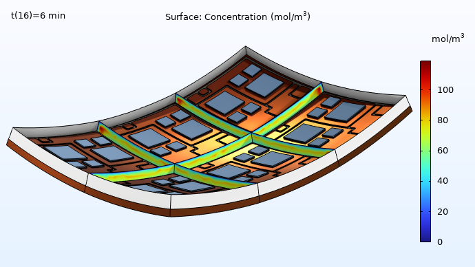
Stress distribution when the temperature peak for the reflow step is reached at t = 6 min (left) and moisture concentration in the plastic seal when the temperature peak for the reflow step is reached after t = 6 min, with the structure deformation shown (right).
An animation of the structure deformation during the reflow step (3 cycles).
Further Testing
Modeling the deformation that occurs during the preconditioning process provides engineers with a better understanding of the impact on the IGBT’s module, allowing them to subsequently modify their designs to avoid damage and improve yield and reliability. Further testing could extend to heat transfer between the PCB and SMD structures and their surroundings, as well as more complex models that include components such as the viscoplasticity for solder materials.
Next Steps
Learn how to build the preconditioning model by downloading the documentation and MPH-file from the Application Gallery:
Learn more about semiconductors in the electronics industry in these blog posts:

Comments (0)