Semiconductor Devices Blog Posts
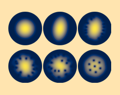
Model Vortex Lattice Formation in a Bose–Einstein Condensate
Bose–Einstein condensation can cause superfluidity, superconductivity, lasers, and trapped dilute cold atoms. When such systems are subjected to rotating perturbation, it forms a vortex lattice.
Computational Electromagnetics Modeling: Which Module to Use?
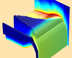
If you work with a particular electromagnetic device or application area, you might be wondering which module in the COMSOL product suite is right for you. Keep reading for a comprehensive intro.
Three Semiconductor Device Models Using the Density-Gradient Theory
You can use the density-gradient theory to model semiconductor devices. Here are 3 examples: a Si inversion layer, Si nanowire MOSFET, and InSb p-channel FET.
Intro to Density-Gradient Theory for Semiconductor Device Simulation
The density-gradient theory is a computationally efficient way to include quantum confinement in the conventional drift-diffusion formulation commonly used for simulating semiconductor devices.
Simulating Radiation Effects in Semiconductor Devices
Analyzing radiation effects in semiconductor devices is an important capability for consumer electronics, medical imaging, nuclear engineering, aerospace, and a wide range of other industries.
Hydrodynamic Thermal Transport in the Kinetic-Collective Model
F. Xavier Alvarez from the Universitat Autònoma de Barcelona (UAB) discusses using COMSOL Multiphysics® to model heat transfer at the nanoscale and better understand transport processes.
How to Simulate the Carrier Dynamics in Semiconductor Devices
Learn how to simulate carrier dynamics in semiconductor devices with 2 examples: reverse recovery and forward recovery PIN rectifier models.
How to Model the Interface Trapping Effects of a MOSCAP
Looking to analyze interface trapping effects in a MOSCAP? Learn how to use a feature in the Semiconductor Module that enables you to add charging and carrier capture/release effects to a model.