
Have you ever wondered how to import the geometry of a printed circuit board (PCB) into the COMSOL Multiphysics® software and prepare it for meshing and analysis? Version 5.3 of the COMSOL® software has the tools to generate geometric objects from the 2D layouts of ECAD files, group them into easy-to-use selections for simulation setup, and automatically take care of the geometric complexity inherent to ECAD formats before meshing. We also have a new tutorial model to demonstrate this functionality.
File Formats for Printed Circuit Board Fabrication Data
In the early days of PCB design, we had to manually create photomasks for the copper layers by laying out shapes for traces and pads on clear sheets — for example, by using self-adhesive tape or rub-on shapes. Nowadays, the layouts for photomasks are created in ECAD design software and the fabrication data is transferred digitally to the manufacturer.
![]()
Before ECAD design software, photomasks had to be manually created in order to design PCBs. Image by Peellden — Own work. Licensed under CC BY-SA 3.0, via Wikimedia Commons.
There are several file formats for this purpose, and the ECAD Import Module supports one of the most widely used options: the ODB++® format. ODB++® format is a compressed archive of the various files that contain PCB fabrication data. Another widely used format in the industry is the Gerber format, which is supported for import into the COMSOL Multiphysics software through the conversion software NETEX-G, available from Artwork Conversion Software, Inc.
The New Kid on the Block: IPC-2581
A recent addition to the available file formats for PCB fabrication data is the IPC-2581 format, which was introduced in 2004. Maintained and developed by the IPC-2581 Consortium, the format is an open standard that defines a single XML-based file to contain all necessary information for the PCB fabrication. This information includes the copper layouts, layer stack-up and drill information, electrical connectivity and component data, the bill of materials, and other data. While IPC-2581 is still young when compared to the other major formats (the original Gerber format was introduced in 1980 and the original ODB++® format in 1995), we have seen it gain acceptance and support from both ECAD design software and PCB manufacturers.
While it is not yet possible to import IPC-2581 files via the ECAD Import Module (as of publishing this blog post), COMSOL has recently joined the IPC-2581 Consortium and support for the IPC-2581 format can be expected in a future version of the COMSOL software.
Editor’s note, 8/17/18: The ECAD Import Module supports the import of the IPC-2581 PCB format as of version 5.3a of the COMSOL Multiphysics® software.
Generating the PCB Geometry from the Layout Data
Regardless of the file format of the fabrication data, the 2D copper layout from a data file is reminiscent of the clear sheet with the attached shapes used in early design methods. The difference is that instead of a real “collage”, the designer creates a digital collage of shapes that builds up the traces and pads on the layer.
During the import, the first steps of generating a geometry for simulation with COMSOL Multiphysics are to import the individual shapes from the layout data and then combine them into connected geometric objects. During this process, interior edges are automatically eliminated to reduce the complexity.

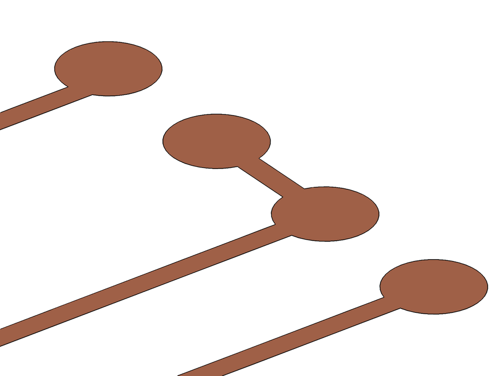
The figure to the left shows circular shapes representing pads and rounded rectangles representing the copper traces in the ODB++® file. To the right, the same region of the layout is shown after the generation of a geometry without interior edges. The file is provided through the courtesy of Hypertherm, Inc., Hanover, NH, USA.
The resulting objects can still contain short edges, for example, if the imported data contains segmented circular edges. We can easily eliminate these by using the Remove Details operation, which can automatically find short edges and either collapse them or merge them if the requirement for tangency is fulfilled.
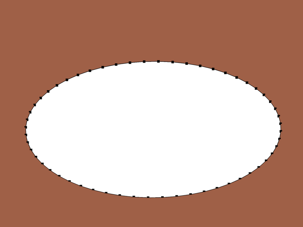
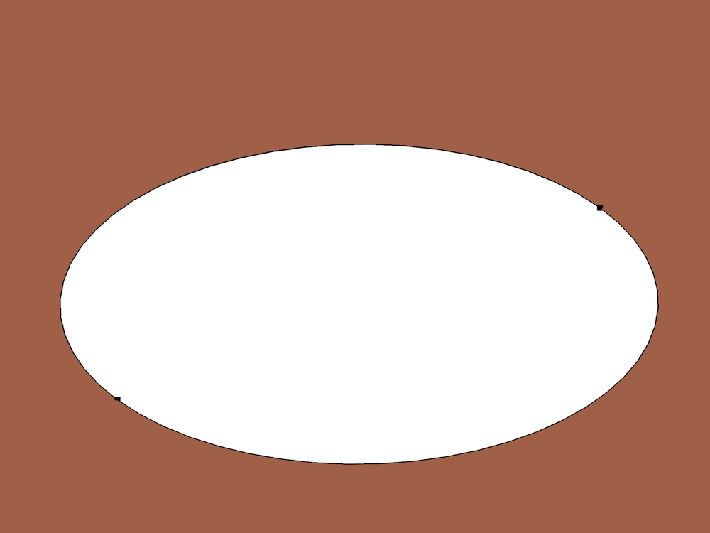
The segmented edges of a hole in a copper layer in the image to the left are joined together in the image to the right after applying the Remove Details operation, which can automatically detect and merge these segments. The file is provided through the courtesy of Hypertherm, Inc., Hanover, NH, USA.
By getting rid of these short edge segments, we gain better control over the meshing process. The mesh elements no longer have to respect the points between the edges. Instead, we can freely adjust the mesh element size to let the mesh elements resolve the hole boundary of choice.
When selecting an ODB++® file for import, the layer thickness and elevation information is read from the file and displayed in the Settings window for the import. We can edit this data and even import it from a previously saved text file. During the import, the selected 2D copper, dielectric, and drill layers are extruded according to this information. It is easy to turn off the extrusion of the copper layers by changing the Type of import setting to Metal shell from the default Full 3D. This can come in handy for simulations for which the copper layer can be modeled as a shell geometry. You will not have to spend time changing the individual thickness values to zero.
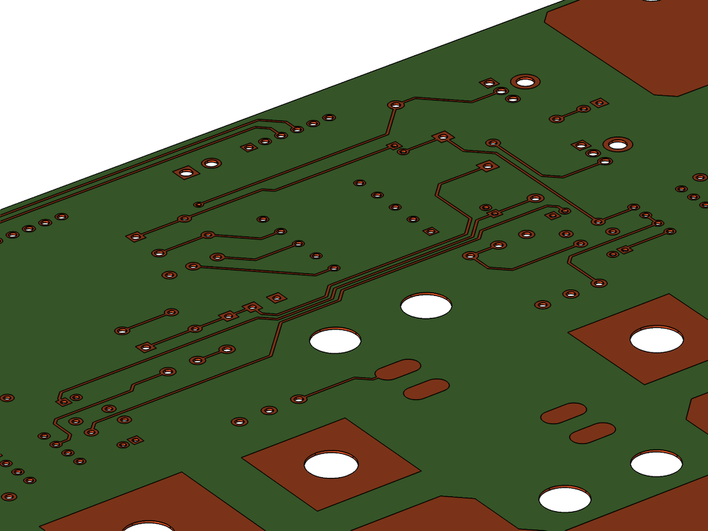
A partial view of the two-layer PCB geometry. The file is provided through the courtesy of Hypertherm, Inc., Hanover, NH, USA.
Use Selections for Faster Model Setup
PCBs are usually built up by many copper and dielectric layers. Setting up physics is quite tedious if we have to manually select geometric entities when setting up the simulation, for example, to assign a certain mesh size to some of the copper layers that consist of many faces. To make this process more efficient, the import defines selections for the different layers. These selections are available both for downstream geometry operations and for defining materials, physics, and even mesh settings.
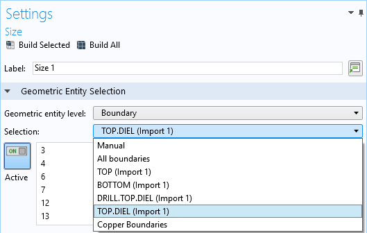
Selections defined by the Import operation appear automatically in the Settings window for a Size attribute in the meshing sequence.
Try It Yourself
The ECAD Import Module includes a new tutorial model called Importing and Meshing a PCB Geometry from an ODB++® Archive. The model shows how to import data from an ODB++® file, generate the geometry of the PCB, and set up a mesh. Layouts imported with the ECAD Import Module can be used for any type of analysis in COMSOL Multiphysics: electromagnetics, structural, acoustics, heat, fluid flow, chemical, or combinations of these. Give it a try!
Support for implementation of the ODB++ Format was provided by Mentor Graphics Corporation pursuant to the ODB++ Solutions Development Partnership General Terms and Conditions (http://www.odb-sa.com/). ODB++ is a registered trademark of Mentor Graphics Corporation.


Comments (0)