The dielectric slab waveguide is one of the conceptual building blocks in photonic structure design. Although most real structures are more complex than just a two-dimensional dielectric slab, we can still learn a lot about modeling from this case. Here, we will look at the case of a small lossy scatterer in the proximity of an optical waveguide, show how this interacts with the fields, and compute reflection and transmission along the waveguide, as well as losses and scattering.
Background
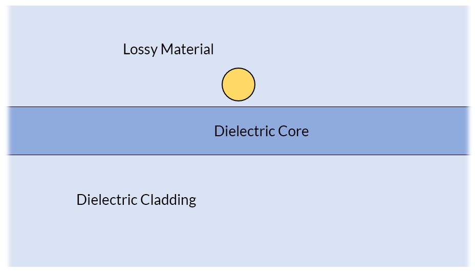
The schematic of the example case is shown below. A dielectric slab waveguide has a small circular metallic object nearby that will interact with the fields, lead to some losses within the material, and cause scattering of light into all directions. For the example of a waveguide without the nearby object, this case would reduce to a perfect dielectric slab waveguide, which is discussed in this model.

Schematic of a 2D dielectric slab waveguide with a lossy material in proximity to the core.
We will consider the case of a waveguide that is wide enough to support multiple modes, although we will restrict ourselves to just the example of the electric field polarized out of the modeling plane. (We can reasonably assume that either the electric or the magnetic field is polarized purely out-of-plane, and that there is no coupling between these two, as long as all materials are isotropic.) This simplifies our analysis a little bit.

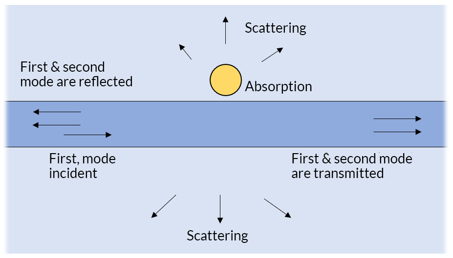
The incident light guided along the waveguide can be reflected, transmitted, absorbed, and scattered.
Before starting our modeling, it is worth doing a bit of manual bookkeeping, thinking of where the light is coming from, and where it is going. We will consider light propagating along the waveguide toward the scatterer, and that this incident light is the first, fundamental, mode. Due to the scatterer, some fraction of the incident light will be:
- Transmitted forward and of the same fundamental mode
- Transmitted forward, but converted into the second mode
- Reflected backward, and into the fundamental mode
- Reflected backward, and into the second mode
- Absorbed by the lossy metallic inclusion
- Scattered into other directions
Computing the transmission into the four possible guided modes of the waveguide (items 1–4) requires solely that we introduce four different numerical ports into the model, two on either side. As already discussed in a previous blog post, it is possible to introduce multiple interior slit port boundary conditions at boundaries within the modeling space. Modeling the absorption into the lossy material simply involves integrating the loss within the metallic object. It is the last quantity, the computation of the scattered light, that requires some special attention.
Computing Scattered Light
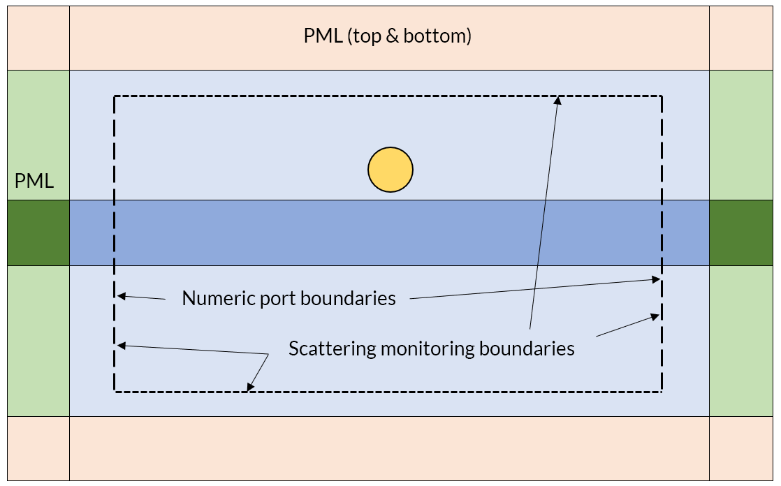
In general, the scattered light from the object near the waveguide can go in any direction. We do know, however, that light propagating along the axis of the waveguide must be one of the guided modes. So, if we draw a boundary normal to the propagation direction of light within the waveguide and integrate the power flow crossing this boundary, we know that this integral will be the sum of the guided light plus whatever scattered light is propagating nearly but not exactly parallel to the waveguide. The light that is guided along the waveguides is computed by the port transmittances and reflectances. So if we subtract this away, we are left with the scattered fraction. Now, since we are integrating across an interior boundary, we will want to make use of the up() or down() operators to evaluate the flux only on one side of the boundary. To integrate these accurately, we use a boundary layer mesh.
We can insert additional interior boundaries that are tangential to the waveguide, and also monitor the power flow across them. They will form a rectangular box along with the previous two boundaries. Integrating the power flowing out of this box gives us the total of all scattering and all light leaving as a guided mode.

Schematic of our computational model.
Along with monitoring the scattered light, we also need to make sure that the light that is propagating out of the modeling domain does not get reflected back. We do so via the usage of perfectly matched layers (PML), which do a very good job of absorbing most outgoing radiation with their default settings. However, for the PML’s adjacent to the waveguide, we can get a little bit better performance by adjusting the characteristic wavelength in the PML settings to be based upon the propagation constant of the first guided mode of the waveguide, because we do know that most of the power is still carried in this mode. This setting is shown in the screenshot below.

Manual adjustment of the PML wavelength settings.

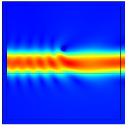
Sample results showing a lossy metallic scatterer near a dielectric slab waveguide.
The results of our model are shown in the image above, and the model file is available for download via the link below. Whenever you are modeling a scatterer near a dielectric waveguide you will want to use the combination of modeling techniques developed here.
Try It Yourself
Get the model discussed in this blog post by clicking the button below, which will take you to the Application Gallery.


Comments (6)
Tesfay Abraha
September 1, 2020Thanks. very nice program
Andre Hagley
January 12, 2021Thanks Walter, this looks like exactly what I need. Can this be done with counter-propagating modes to evaluate a coupled mode calculation?
Andreas Maeder
June 23, 2021Is it correct that I get an absorption value of around 0.5 and negative scattering in x direction? If so, what does the negative scattering mean? Is this (unwanted) scattering from the PML back into the domain?
Also I noticed that in the last picture there is no field to the left of the input port, however if I run the file on my computer, I also get some light there.
Henrik Parsamyan
August 15, 2021Dear Walter,
Thank you very much for this article, it is super helpful.
This example gives results for the electric field polarized out of the modeling plane. How can I set up the model to study the magnetic field polarized along out-of-plane direction?
Thank you in advance.
Дмитрий Жабровец
October 5, 2024Thank you for the article. Please answer my question. I am trying to do something similar, but instead of a circle I have a silver film. I will check how the plasmon resonance effect polarizes the radiation, that is, both TE and TM modes are important here. When I model the waveguide in the longitudinal direction, I manage to get the fundamental mode, but it is polarized only in one direction (in z), although it should be polarized in z and y. In the listed examples, as well as other examples on the site, everywhere during the modeling the light is polarized only in the z direction, although when modeling the waveguide in the transverse direction it is possible to find both TE and TM modes
Evan Sisler
December 12, 2024 COMSOL EmployeeHi! Thank you for your comment.
For questions related to your modeling, please contact our Support team.
Online Support Center: https://www.comsol.com/support