
In this blog post we will explore the “last frontier” of the electromagnetic spectrum: the terahertz band. We will look at how the Semiconductor Module and RF Module, add-on products to the COMSOL Multiphysics® software, can be used to create a simple yet powerful model of a photoconductive antenna (PCA), a common device in terahertz engineering.
Introduction to the Terahertz Band
The spectrum of electromagnetic waves spans roughly 15 orders of magnitude in frequency, and humankind has managed to harness nearly all of it in applications such as long-range communications and cancer treatments. Even so, the terahertz band (frequencies ranging from roughly 0.1 THz to 10 THz), often called the “last frontier” of the electromagnetic spectrum, has eluded large-scale application due to technical challenges related to production and detection of terahertz waves — until recently. The last decades have seen remarkable advancements in technological innovation related to the creation and detection of terahertz waves, and it seems that commercial applications of the THz band will soon become commonplace. In fact, the frequency of operation of 6G technology may fall in the terahertz range.
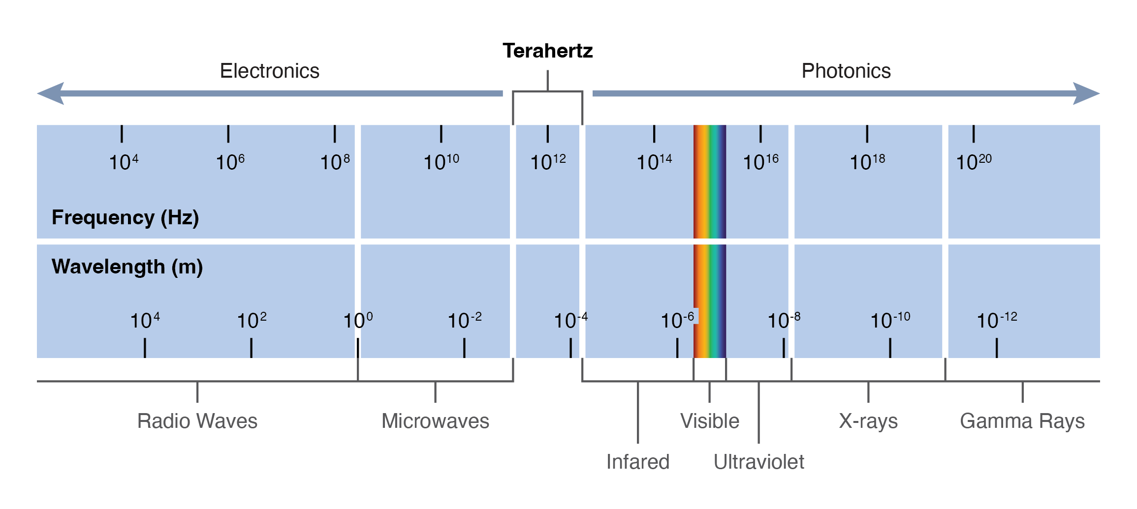 Figure 1. The terahertz spectral range lies between the microwave and the infrared ranges.
The attractiveness of the THz band is not simply a matter of achieving higher bandwidths with larger frequencies. Many materials such as fabrics and cellulose do not absorb terahertz radiation very strongly, so THz imaging can be used to see through clothing and packaging materials. On the other hand, since many molecules have rotational and vibrational states with energies in the terahertz band — and thus do strongly absorb THz radiation — it’s possible, given the correct setup, to obtain accurate information of chemical composition from a THz image. Moreover, THz waves are nonionizing and thus safe to humans. For these reasons, THz imaging is a highly desirable alternative to X-rays for applications such as security screening.
One component that is a basic building block in many THz devices is the PCA, which is why modeling a PCA will be the focus of this blog post. We will explore how to use the Semiconductor Module and RF Module to create a PCA model that can predict the THz emission spectrum and directivity of the device. While a PCA can be used for both generating and detecting THz waves, for simplicity we will focus on the case of a PCA emitter. The setup adopted here is based on Ref. 1.
How Does a PCA Work?
The principle of operation of a PCA is fairly straightforward. A DC bias voltage is applied between conductive terminals on a substrate made of a low-conductivity semiconductor, such as low-temperature GaAs (LT-GaAs; this is produced when the gallium arsenide, or GaAs, has been crystallized at low temperature, yielding a large concentration of crystal defects). The gap between the terminals is then illuminated with a fast pulsed laser. Provided that the photon energy of the laser is greater than the band gap of the semiconductor, the laser pulse causes generation of electron-hole pairs, increasing the conductivity rapidly. A transient pulse of current, known as the photocurrent, flows between the terminals, leading to the generation of a pulse of electromagnetic radiation. If the laser pulse duration is in the femtosecond range, the spectrum of this pulse will generally fall in the terahertz band. As soon as the laser pulse ends, rapid recombination of the carriers occurs, mediated by the high defect concentration. The recombination leads to an exponential decay of the current density. A schematic of the PCA is shown in the figure below.
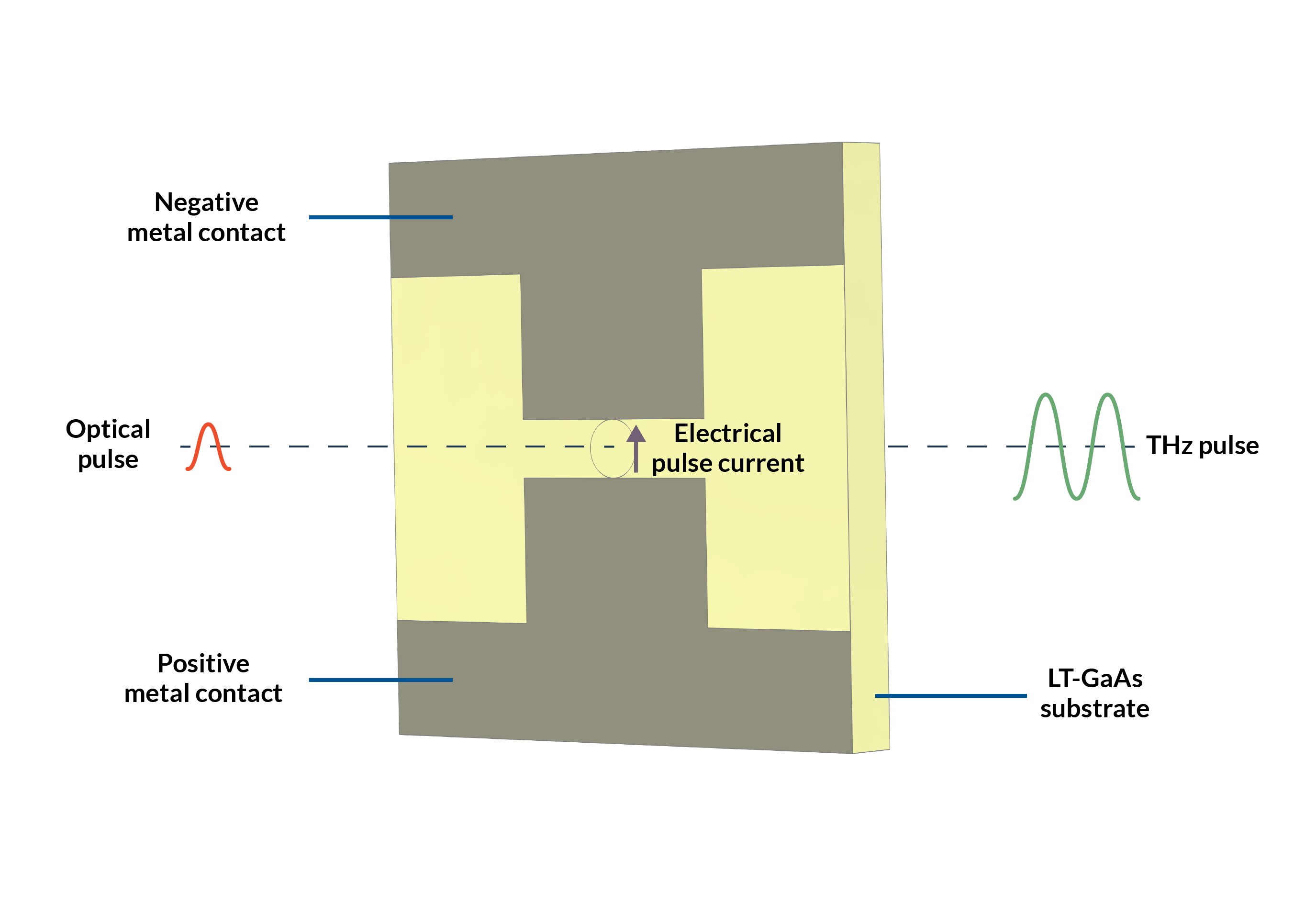 Figure 2. The PCA in emission mode.
Modeling the PCA with COMSOL®
For this modeling application, the Semiconductor interface in the Semiconductor Module is used to obtain the transient current density that results from the laser pulse, and the Electromagnetic Waves, Transient interface in the RF Module is used to simulate the generation of the THz pulse. The setup is depicted in Figure 3. To minimize computation time, we use two 2D components. In Component 1, we first solve for the current density in the xz-plane such that the current will mainly flow in the z direction. (The coordinates of this component are still x and y by default, and the current will flow in the y direction. Component 1 will be mapped to Component 2 as explained below.) Then, with Component 2 we simulate the propagation of the resulting THz wave in the xy-plane so that the source current density can be applied perpendicular to the plane of the model.
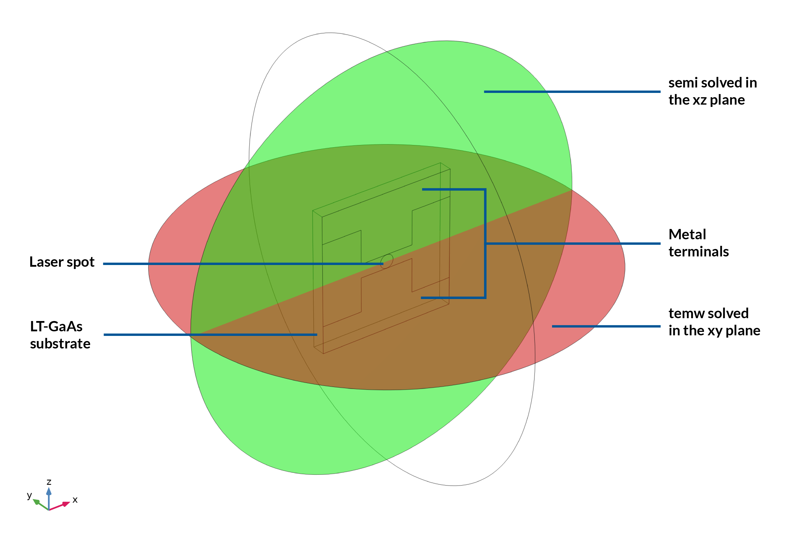 Figure 3. Geometry used for the PCA model. The photocurrent is solved for in the xz-plane (green) using the Semiconductor interface (semi, in the image), whereas the transient THz pulse is modeled in the xy-plane (red) using the Electromagnetic Waves, Transient interface (temw, in the image). The photocurrent density is applied as a boundary source current density along the line of intersection of the xz-plane and the xy-plane.
Semiconductor Interface Settings
Let’s first take a detailed look at how to model the carrier dynamics of the PCA using the Semiconductor interface in Component 1. Adopting the 2D approach means that we assume the laser pulse to decay extremely fast inside the GaAs substrate so that there is no need to resolve the photocurrent in the y direction, and the parts of substrate covered with the terminals can be removed from the domain of the simulation. For the purposes of scaling, we set the out-of-plane thickness to 1 µm. In addition to setting up two metal contacts as shown in Figure 3, we need to add an Optical Transitions node to model the generation of electron-hole pairs due to the laser pulse. We opted for a simple Gaussian distribution for the E-field amplitude in both space and time. The beam radius was set to 5 µm to match the gap size, whereas the temporal pulse width (standard deviation of the Gaussian function) was set to 100 fs with a 0.5 ps delay. Finally, we need to account for the fast recombination process mediated by the large concentration of crystal defects (i.e., traps) of LT-GaAs by including a Trap-assisted Recombination node and specifying the carrier lifetimes. The material properties used were based on Ref. 1. The time-dependent simulation was run for 5 ps to sufficiently capture the tail of the recombination process.
The main result we obtain from the semiconductor simulation is the transient photocurrent density between the terminals. To apply this as a boundary source current density along the line of intersection of the two geometries in Component 2, we need to set up a Linear Extrusion Operator. After specifying the appropriate end and starting points in the respective geometries, we can map any variable of Component 1 to Component 2 by using the _comp1.linext1()_ operator.
Electromagnetic Waves, Transient Interface Settings
Now that we have obtained the photocurrent, we can move on to simulating the THz pulse itself using the Electromagnetic Waves, Transient interface in Component 2. The geometry of this component consists only of the cross-sectional slice of substrate (we assumed the total substrate thickness to be 5 µm) surrounded by a circular domain of air. Since the source current will flow in the out-of-plane direction, we can make the computation more efficient by solving only for the out-of-plane component of the E-field. To suppress unphysical reflections, we apply the Scattering Boundary Condition feature on the exterior boundary. To obtain the far-field spectrum, we need to add a Far-Field Domain node (this needs to be accompanied by the Time to Frequency FFT study step), applied only to the air domain, with the far-field calculation performed at the exterior boundary of the model. Finally, we use a Surface Current Density node to apply the photocurrent mapped from Component 1 as a current source. To make sure that we get sufficient resolution in the frequency domain, we run this study for 10 ps rather than 5 ps like for the semiconductor part.
For the study settings, we need to first perform a time-dependent study to simulate the propagation of the THz pulse. For computing the far-field spectrum, the time-domain data must be transformed to the frequency domain using a Time to Frequency FFT study step.
The Results
Let’s first take a look at the results of the semiconductor calculation. Figure 4 shows an animation of the generation rate density of electron-hole pairs due to the laser pulse, the electric field, and the current density during the first 2.5 ps of the simulation. Furthermore, Figure 5 shows a 1D plot of the terminal current and the total generation rate. It can be seen that the photocurrent decays more slowly than the generation rate due to the pulse duration being much shorter than the carrier lifetimes.
Figure 4. From left to right, the generation rate density, the electric field, and the electric current density during the first 2.5 ps of the semiconductor simulation.
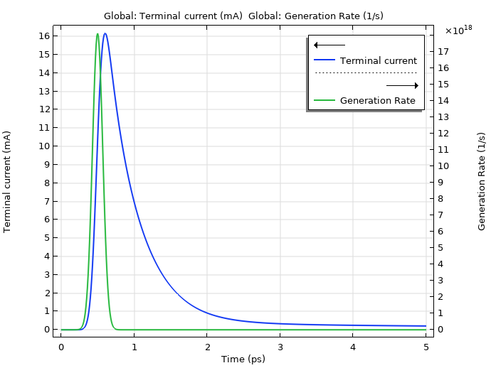
Figure 5. The time dependence of the terminal current and the total generation rate. The peak power of the laser pulse is attained at 0.5 ps.
Let’s now take a look at the THz pulse itself. The animation in Figure 6 shows how the pulse propagates away from the PCA. The source current density is shown as a line plot on the surface (bottom boundary) of the substrate. In Figure 7, we plot the pulse waveform at two different points. From these plots we can see how the reflections from the substrate cause extra ripples after the initial wavefront.
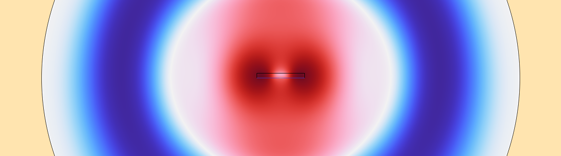
Figure 6. The source current density plotted on the bottom boundary of the substrate and the outgoing THz pulse it generates. The circle has a radius of 250 microns.
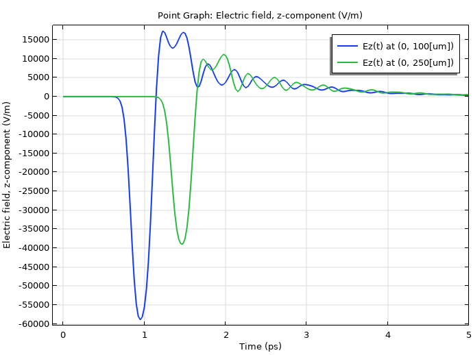
Figure 7. The electric field (Ez) 100 and 250 µm away from the PCA.
Finally, we have a plot of the far-field spectrum of our PCA obtained by combining the Far-Field Calculation node with the Time to Frequency FFT study. We find that the pulse has the strongest peak at approximately 0.75 THz but with significant power all the way up to nearly 5 THz. Additionally, we see slight directivity due to the substrate when we compare the far-field spectra in the forward (y direction) and sideways (x direction) directions.
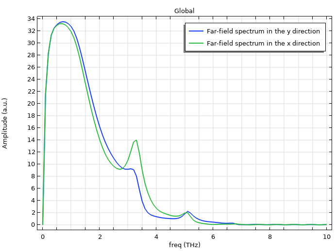
Figure 8. The far-field spectrum of the THz pulse obtained using the Time to Frequency FFT study. We can see slight directivity due to the presence of the substrate when comparing the spectrum in the y direction and x direction.
We should note that this simple approach to modeling a PCA comes with some limitations:
- We have assumed that the laser intensity inside the GaAs substrate decays sufficiently fast to allow 2D treatment, so we cannot resolve the photocurrent density in the z direction.
- We only simulated the THz pulse in the plane between the terminals, so the effects that the metallic terminals have on the pulse spectrum and directivity are ignored. This also means that the antenna shape has not been optimized for the calculated THz bandwidth.
- Our simple model only includes a thin substrate, which is not sufficient to provide strong directivity. A more realistic model should include a thicker substrate domain and/or silicon hyperhemisphere lens to direct the THz beam.
These limitations can be overcome with a full 3D model that accounts for the antenna geometry in the THz pulse simulation.
Conclusion
In this blog post, we explored how the Semiconductor Module and RF Module can be used to model THz devices from first principles by building a simple model with real predictive power. The model shown here simulates the spectrum and directivity of the THz emission from a PCA. You can download this PCA model and try it yourself by clicking the button below!
Reference
- J. Zhang et al., “Numerical analysis of terahertz generation characteristics of photoconductive antenna,” 2014 IEEE Antennas and Propagation Society International Symposium (APSURSI), pp. 1746–1747, 2014; https://ieeexplore.ieee.org/document/6905199.
Further Learning
- To learn more about working in the terahertz regime, check out this archived webinar on simulating THz metamaterials:

Comments (1)
Matiullah Khan
June 20, 2024I love to join these courses