
In 1870, an audience watched as a stage was set with two buckets, one on top of the other. Due to a small hole in the upper bucket, water poured into the lower bucket, bending as it did so. To the audience’s amazement, sunlight followed the bend of water — a phenomenon later termed total internal reflection. The performer on stage, John Tyndall, was one of the many scientists who tried to control the most visible form of energy: light.
Entering the Era of Photonics
For decades, researchers aimed to find a way to control light and use it for the transmission and processing of information, an area of study known as photonics. In the meantime, electrons took this responsibility on their shoulders. More recently, scientists were able to viably manufacture nanostructure devices and control the flow of light, due to the extensive development of technologies such as photolithography, molecular beam epitaxy, and chemical vapor deposition. The packets of light (photons) were projected as a prospective candidate to assume the responsibilities of sustaining Moore’s law.
The Beginning of the Photonic Integrated Circuit
The goal of researchers studying photonics was to deliver an analogue of an electronic integrated chip that could perform all of the required computational processes using photons while being space and time efficient. Scientists termed this technology photonic integrated circuit (PIC), devices that could integrate different optical components on a single substrate. This chip should, in principle, be able to perform various optical operations, such as focusing, splitting, isolation, polarization, coupling, modulation, and (eventually) detecting light.
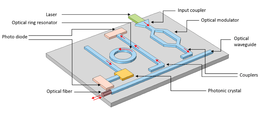
Schematic of the photonic integrated circuit (not to scale), showcasing different optical components. For more information, see Ref. 1.
In this blog post, which is the first in a new series on silicon photonics, we discuss optical waveguides. Later in the blog series, we will contemplate how these optical components came to be an inevitable part of PICs.
Developing Optical Components for PICs
The different optical components constituting a fully functioning PIC were subject to research. Scientists determined that the way to create the light source was through lasers, which could deliver a narrow-band light source to the integrated chip component. As for optical fibers, they could transport light from one end to the other for thousands of kilometers. Then there was the most common component in a PIC: the optical waveguide. This waveguide could link different components on the substrate.
Input couplers were developed to efficiently couple the light from lasers or optical fibers to the optical waveguide placed on the substrate, while directional couplers were created to control the coupling of light between two parallel optical waveguides. Then came the ring resonator, which served the same purpose as an optical filter (that is, allowing only a narrow band of frequency) and could also couple two optical waveguides in opposite directions.
An example of an optical ring resonator notch filter.
Negotiating Nonlinear Effects
Some scientists probed the much underappreciated nonlinear optical effects to devise second-harmonic and third-harmonic waves. With these waves, it would be possible to perform operations between two optical beams, such as frequency doubling, differencing, and mixing.
Another invention was optical modulators. These components could modify the light intensity based on the applied DC bias potential using the nonlinear electro-optic effects.
Photonic Crystals: Controlling the Flow of Light
From nature, it was observed that with the periodic arrangement of high- and low-refractive-index materials in 1D, 2D, and 3D, it was possible to reflect a certain band of frequency while allowing another band of frequency to pass. Hence, these materials could act as both a filter and resonator in a certain periodic arrangement. The periodic arrangement of different dielectric materials was termed a photonic crystal.
Finding a Material to Propagate Light
With the idea of creating optical waveguides to propagate light on chip-scale packages, scientists were left to wonder which materials to use. One of the materials was high-refractive-index GaAs. This was used as the core and was surrounded by low-refractive-index AlGaAs. More advanced techniques were developed to dope titanium in the lithium niobate substrate to increase its refractive index and form a core.
The focus was narrowed down to silica, which is more easily available than any other material. The technology came to be known as silica on silicon (Si-SiO2) or silicon on insulator (SOI), where the silicon (high refractive index of ~3.5) was embedded within silica (lower refractive index of ~1.4). The fabrication techniques for silicon were well established (courtesy of electronic chips) and at the same time, silicon was compatible with other CMOS techniques, which helped boost research into silicon photonics technology.
Different Configurations of Silicon Waveguides
The crux of the silicon waveguide lies with the high contrast of the refractive index, around a 50% difference. Prior work relied on total internal reflection to confine the energy. In this case, energy was confined in a higher-refractive-index core that was surrounded by a low-refractive-index cladding. However, recent work confined the energy in the lower-refractive-index slot neighbored by the high-refractive-index slabs, inherently helping to lower losses.
Guiding Light in a High Refractive Index
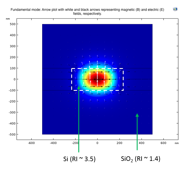
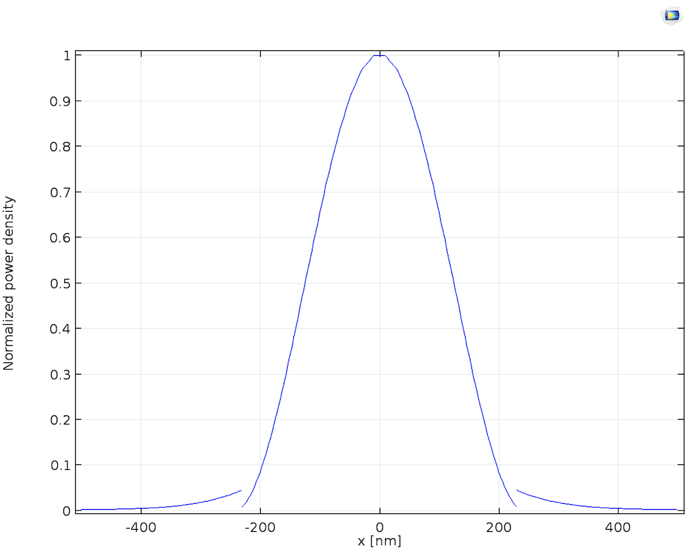
The first technique involved confining the energy in a higher-refractive-index medium, where the inner core (in the order of hundreds of nanometers) is devised with a high-refractive-index material (silicon) surrounded by a low-refractive-index cladding (silica). The difference in the refractive index must be as much as 50%.
The fundamental mode is confined in the core, as shown in the image below on the left, and the confined normalized power, as shown in the image below on the right.
Left: The fundamental mode for an operating wavelength of 1.55 um. The white and black arrows depict the magnetic and electric field. Right: The normalized power density through the center of the waveguide.
Guiding Light in a Low Refractive Index
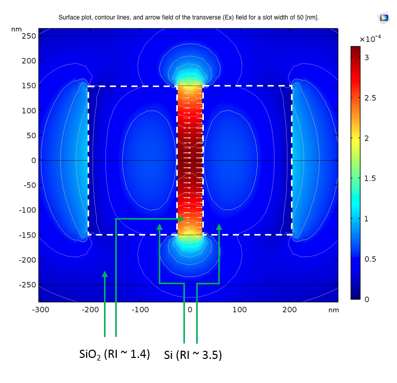
Although counterintuitive, the energy could also be trapped in a low refractive index. Moreover, it was found that more energy stays put in an even and narrow region (20 to 80 nm), which makes a low refractive index more compatible for integration with photonic circuits.
Such a design involves two slabs of high refractive index neighboring a nanoslot of low refractive index. Further, considerable energy is bounded in the slot.
Left: The transverse (Ex) field for a slot width of 50 nm. Right: The normalized transverse electric field (Ex) through the center of the waveguide.
To analyze the required width of the nanoslot for delivering maximum power through the waveguide, it was imperative to perform a sweep of the width, as shown below.
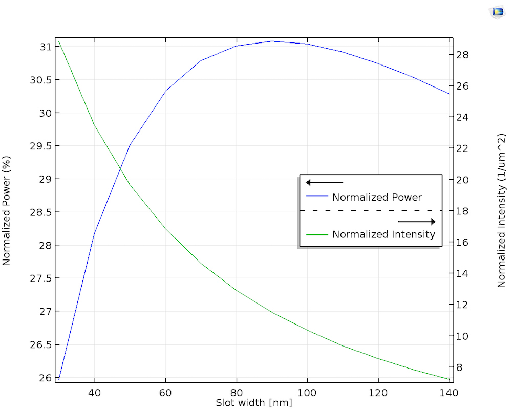
The normalized power and intensity in the slot versus slot width.
Designing and Prototyping Silicon Waveguides
Fabricating such an optical waveguide prototype and then analyzing it is resource intensive. An alternate, preferred approach is to use numerical tools such as the COMSOL Multiphysics® software. With this simulation tool, one could quickly set up prototypes and investigate further before finalizing the prototype to be fabricated.
We can use COMSOL Multiphysics to perform a mode analysis on the 2D cross section of the silicon waveguide (both for high- and low-refractive-index cases). This enables us to evaluate the effective refractive index of the waveguide and the fundamental mode, which helps us understand the normalized power distribution.
We implement the full 3D propagation for both types of waveguides by first having a 3D geometry of the optical waveguide and assigning Numeric Port boundary conditions on both ends of the waveguide. The Boundary Mode Analysis study (similar to a mode analysis in 2D) could be applied on these numeric ports to figure out their fundamental mode. The fundamental mode could be used to propagate within the waveguide using the Frequency Domain study, as shown in the animations below.
The y-component of the H-field propagating in the high-refractive-index confinement case for a silicon waveguide with a length of 10 um.
The y-component of the E-field propagating in the low-refractive-index confinement case for a silicon waveguide with a length of 10 um.
Final Thoughts on Silicon Waveguides
This is the first blog post in the Silicon Photonics blog series, where we will discuss different optical components in detail and how a finite element analysis tool such as COMSOL Multiphysics can help design these components. On our journey from laser cavities to photodetectors, we will meet some fascinating scientists and discuss how they attempted to control light.
Stay tuned!
Try It Yourself
Check out these tutorial models on silicon photonics:
Updated List of Blog Posts in the Silicon Photonics Series
References
- B.E.A. Saleh and M.C. Teich, Fundamentals of Photonics.
- K. Yamada, “Silicon Photonic Wire Waveguides: Fundamentals and Applications”, in Silicon Photonics II, 2011.
- V. Almeida, Q. Xu, C. Barrios, and M. Lipson, “Guiding and confining light in void nanostructure”, Optics Letters, vol. 29, pp. 1209–1211, 2004.



Comments (23)
Rishabh Bhatia
June 17, 2018I need help in designing the optical cable with a nanoparticle attached at its one end and study the effect of passing a laser through it. Is there any procedure to follow to accomplish this?
I was thinking of drawing two separate geometries:-
1- A spherical nanoparticle
2- An optical fiber cable
Then I can attach the two models together.
Can anyone guide me through the procedure to follow for it?
Uttam Pal
June 21, 2018 COMSOL EmployeeHi Rishabh, I believe you initially you can start with a 2D approximation of your dielectric waveguide (https://www.comsol.com/model/14709) and then introduce the nanoparticle within this waveguide itself. To know how to launch the laser in 2D, you can go through this Beam splitter (https://www.comsol.com/model/31041). To extend this discussion, I believe support@comsol.com would be the best avenue.
Rishabh Bhatia
June 26, 2018Thank you for your help.
I wanted to know is there any possible way to draw a structure of astroid in 2-d and then extrude it to form a 3-d structure. Or is there any e=way to directly draw structure like that?
For example- I want to draw a structure of a prism in which I can manipulate its edges to be curvy and at the same time it should have a tip (which should behave as a point) and from that tip and the structure of that polygon or pyramid or prism enhances with distance.
Subhash Arya
August 11, 2018We are not able to see/watch the video attached with this blog.
Uttam Pal
August 15, 2018 COMSOL EmployeeDear Subhash, we would recommend you to download or update Adobe flash player in your current PCT and then you should be able to see the video. We are able to see the video at our end.
Rui Ma
November 6, 2018Hi. Could you please tell me how to set the animation of 3D silicon waveguide in Comsol, or could you please upload the demo of this simulation work?
Uttam Pal
November 6, 2018 COMSOL EmployeeDear Rui,
The 3D animation of the silicon waveguide is very much similar if you do the following steps in the Waveguide Adapter #140 model file.
Step 1: Run the model for a single frequency (i.e in Frequency domain study).
2. Right click “Export >> Animation >> Player”.
3. Choose “Animation >> Subject >> Electric field”.
4. Choose “Animation >> Settings >> Sequence type >> Dynamic data extension”. This enables the phase dependent frames data.
5. Play and export.
Madhusudan Mishra
November 15, 2018Dear Pal,
Can you please provide me the steps how you have simulated this? I have done 3d simulation of silicon waveguide (BaTiO3 cladding) but I am unable to find
1. the waveguide loss and
2. Light and cladding overlap factor for say TE00 mode.
Uttam Pal
November 15, 2018 COMSOL EmployeeDear Madhusudan,
The best place to pose the question regarding your model will be support@comsol.com. There we can give you in-depth response.
Arif Hossan
November 17, 2018Dear Uttam,
I am trying to propagate light through 3D optical waveguide(like as “Designing and Prototyping Silicon Waveguides”) but I can’t done it.Light becomes splitted.Please help me.
Uttam Pal
December 4, 2018 COMSOL EmployeeHi Arif, now we have uploaded both the models in the “Try It Yourself” section in this blog. The second model showcase the approach to model 3D optical waveguides.
Madhusudan Mishra
December 24, 2018Dear Pal,
Thank you for your response. Can you please provide the pdf containing the steps for doing the 3d optical WG simulation?
Uttam Pal
December 24, 2018 COMSOL EmployeeDear Madhusudhan,
We don’t have the step by step process for the 3D model. However the approach is exactly same as in “https://www.comsol.co.in/model/dielectric-slab-waveguide-14709” only the geometry is changed.
Uttam Pal
December 24, 2018 COMSOL EmployeeDear Madhusudhan,
In addition to my earlier comment, the major changes from the model #14709 is that the 3D model is using ewbe (Beam envelope) interface and a Physics controlled mapped mesh designed specifically for Beam envelope interface (available only in Wave optics module).
Ahsan Habib
January 24, 2019Gentleman,
I need your help to modelnig a silica high mesa waveguide in my comsol 5.3a. Please give me mph/pdf file for building a general model of high-mesa waveguide, if possible. I’m new in comsol.
Thanks.
Uttam Pal
January 24, 2019 COMSOL EmployeeDear Ahsan Habib ,
The best place to pose a specific question regarding your model will be support@comsol.com, where we can give you an in-depth response.
Marco Mancini
April 27, 2020Hello,
the wave optics module is quite interesting to simulate single components of an optical integrated circuit. However it does not seem to be possible to couple two of these components such as for instance an optical fiber and a waveguide ( input coupler), due to changes in the index of refraction along the direction of light propagation. What do you suggest to study such a simple problem?
Uttam Pal
April 29, 2020 COMSOL EmployeeDear Marco,
People have worked on waveguide-fiber coupler models, many papers are available, however we don’t have an exactly the same example. As of now you would be interested to go through the Focusing lens model (#57621 : https://www.comsol.co.in/model/focusing-lens-57621). Having said that, we are also planning to have a new model showcasing the fiber to fiber coupling model in the next release. Finally, please note that you can use the TBC to model the anti-reflection coating as you can see in the Focusing lens model.
Houman Ghorbani
December 31, 2020Hi Uttam
Does wave optics module simulate a mode effective index and its profile in a bend?
Best!
Uttam Pal
January 8, 2021 COMSOL EmployeeHi Houman,
Yes wave optics can do what you are asking for, please go through the Step index fiber bend model: https://www.comsol.com/model/14189
ANAMITRA GANGULI
February 15, 2021Dear Pal,
I have tried designing the slot waveguide based on the above example.
I need help in designing a directional coupler using Silicon based slot waveguides. I am working on COMSOL for the past couple of weeks and I am new to it. Can you please guide me in modelling the system?
Uttam Pal
February 15, 2021 COMSOL EmployeeDear Anamitra,
The most relevant example to model directional coupler will be https://www.comsol.com/model/14593. This model is also on the lines of slot waveguide configuration. Recommend you go through the documentation which has the step by step documentation. You can also write to support@comsol.com if you have any further technical queries.
Vishwaraj Parrikar
January 24, 2023Hi Uttam. I need help determining whether a waveguide structure supports single-mode or multimode propagation. Could you guide me to accomplish this. Thanks in advance